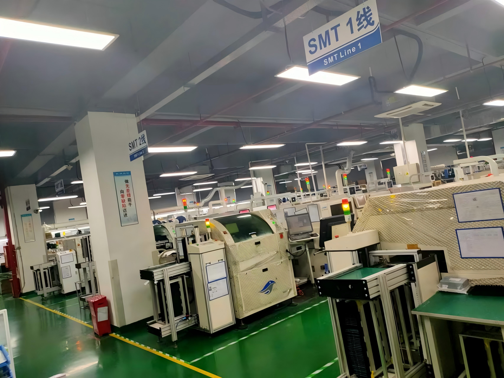
PCB Fabrication
One-Stop PCB & PCBA Manufacturing Service
Professional PCB fabrication, PCBA assembly, components sourcing and full testing, from quick-turn prototype to mass production.
Professional PCB fabrication, PCBA assembly, components sourcing and full testing, from quick-turn prototype to mass production.
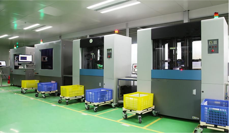
IQC, LDI exposure and impedance control, AOI and X-Ray inspection, functional and final test on every order.
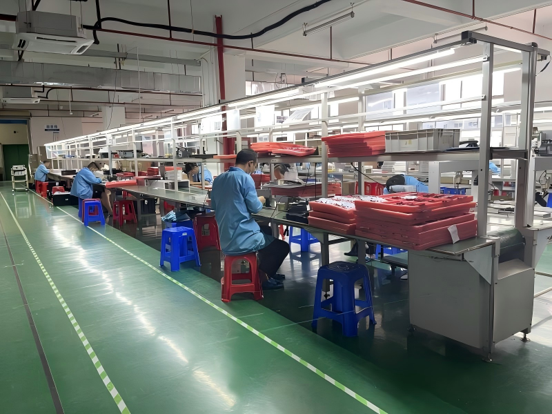
PCB fabrication, components sourcing, SMT and DIP assembly and full testing under one roof.
What we do
PCB fabrication, PCBA assembly, components sourcing and DFM engineering support
Multilayer PCB, HDI, Rigid-Flex, High Frequency, Metal Core and Thick Copper PCB, 1-40 layers.
SMT & DIP assembly, BGA/QFN/CSP soldering, AOI and X-Ray inspection, functional test.
Original components through global authorized suppliers, with fast procurement and cost optimization.
Free DFM analysis, PCB design optimization and professional technical consultation.
Capability at a glance
Key process limits from our PCB production capability, from layer count to tolerance.
Our products
From multilayer boards to fully assembled and tested PCBA
Browse PCB fabrication, PCBA assembly, components sourcing and engineering support.
View All Products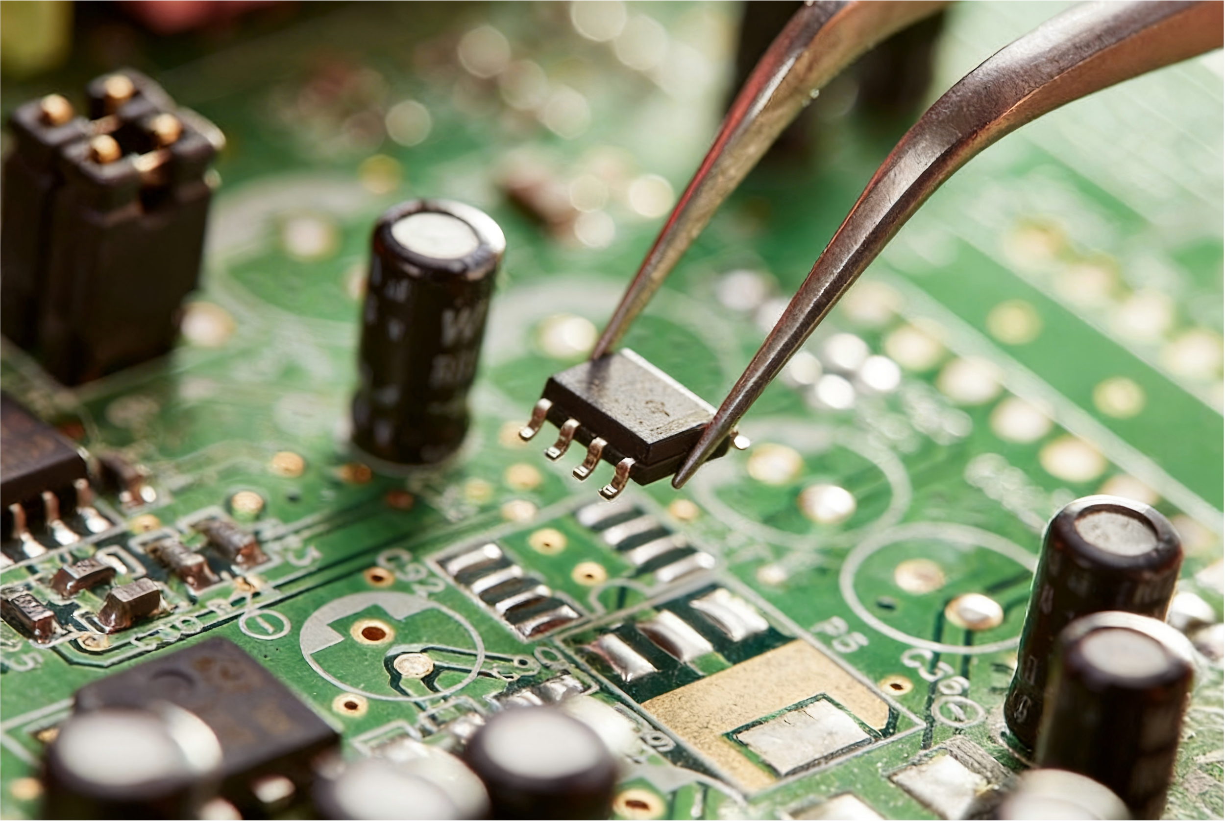
Original electronic components sourced through global authorized suppliers, with fast procurement, cost optimization and alternative-component support.

One-stop PCBA assembly: SMT chip mounting and DIP through-hole assembly, BGA/QFN/CSP precision soldering, AOI and X-Ray inspection, plus functional and aging test.

Free DFM analysis, PCB design optimization and professional technical consultation to improve production yield and reliability before manufacturing.

Rigid-flex and flexible printed circuits for compact, bendable and high-reliability interconnects in medical, automotive and consumer devices.

Aluminum, copper, iron and ceramic base metal-core PCB for LED lighting, power supply and high-thermal applications, from single-sided to 4 layers.

High-density interconnect PCB with blind and buried vias, fine line width down to 3mil/3mil for compact, high-performance electronic designs.
Guides and insights
Buyer guides and technical insights on PCB fabrication and assembly
View More
Why two quotes for the same Gerber files differ: the process decisions behind a PCB and PCBA price, from panel utilization and layer count to finish, testing and lead time.

A practical DFM checklist for PCB buyers and engineers: tolerances, stackup, aspect ratio, surface finish, materials and inspection steps to confirm before you order.

Compare common PCB surface finishes including HASL, ENIG, immersion silver and OSP to match finish to application and assembly needs.